While classical microelectronics relies on homojunctions formed within a single semiconductor host, modern optoelectronics and high-frequency devices exploit heterojunctions—epitaxial interfaces between two chemically distinct semiconductors with different bandgaps and work functions. Bandgap engineering enables the spatial manipulation of conduction and valence band profiles independently.
1. Classification of Heterojunction Band Alignments
When two dissimilar semiconductors A and B are grown epitaxially, the mismatch between their bandgaps (E_{gA}) and (E_{gB}) creates discontinuous energy steps at the interface for both the conduction band ((Delta E_c)) and valence band ((Delta E_v)):
[
Delta E_c + Delta E_v = Delta E_g = |E_{gA} – E_{gB}|
]
Heterojunctions are categorized into three distinct topological alignments:
- Type-I (Straddling Gap): The bandgap of material B lies entirely within the wider bandgap of material A ((E_{c,A} > E_{c,B}) and (E_{v,A} < E_{v,B})). Both electrons and holes are confined within the narrower bandgap material B. Exemplified by ( ext{Al}_x ext{Ga}_{1-x} ext{As} / ext{GaAs}), Type-I heterostructures are the backbone of double-heterostructure laser diodes, high-efficiency LEDs, and quantum wells.
- Type-II (Staggered or Misaligned Gap): Either the conduction or valence band of B is higher than that of A, but not both. For instance, in staggered Type-II (e.g., ( ext{InP} / ext{GaAs}_{0.5} ext{Sb}_{0.5})), electrons localize in one material while holes localize in the other, resulting in spatially indirect exciton transitions with emission energies below either individual bandgap. In broken-gap Type-II (Type-III, e.g., ( ext{InAs} / ext{GaSb})), the conduction band of InAs lies below the valence band of GaSb, creating a semimetallic overlap that enables interband Zener tunneling.
- Type-III (Broken-Gap Alignment): The valence band maximum of one material lies above the conduction band minimum of the adjoining material, producing spontaneous carrier transfer across the interface.
2. Anderson’s Electron Affinity Rule
The simplest quantitative framework for predicting band offsets is Anderson’s Rule, based on the alignment of the microscopic vacuum level (E_{ ext{vac}}). The electron affinity (chi) of a semiconductor is defined as the energy required to remove an electron from the conduction band edge (E_c) to the local vacuum level (E_{ ext{vac}}):
[
chi = E_{ ext{vac}} – E_c
]
Assuming that the vacuum level remains continuous across the metallurgical interface without interface dipole sheets, the conduction band discontinuity (Delta E_c) equals the difference in electron affinities between the two materials:
[
Delta E_c = chi_B – chi_A
]
The valence band discontinuity (Delta E_v) is subsequently determined by energy conservation:
[
Delta E_v = Delta E_g – Delta E_c = (E_{gA} – E_{gB}) – (chi_B – chi_A)
]
Although interface states, strain, and atomic dipole layers introduce corrections to Anderson’s rule, it provides the essential first-principles heuristic for designing heterojunction band profiles.
3. 2D Electron Gas (2DEG) Formation via Modulation Doping
One of the most consequential applications of bandgap engineering is modulation doping, pioneered by Horst Störmer and Raymond Dingle. In an ( ext{n-AlGaAs} / ext{undoped GaAs}) heterojunction:
- Silicon donors are introduced exclusively in the wide-gap AlGaAs layer, separated from the interface by an undoped spacer layer.
- Because (E_{c, ext{GaAs}} < E_{c, ext{AlGaAs}}), donor electrons transfer across the interface into the potential notch on the GaAs side.
- The transferred electrons form a sheet of high-density carriers ((n_s sim 10^{11} – 10^{12} ext{ cm}^{-2})) confined in a quasi-triangular quantum well.
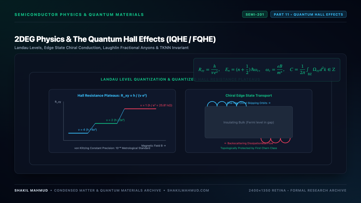
Because these electrons are spatially separated from their parent ionized donor cores in the AlGaAs layer, ionized impurity scattering is virtually eliminated. At cryogenic temperatures ((4.2 ext{ K})), electron mobilities exceed (10^7 ext{ cm}^2/ ext{V}cdot ext{s}), laying the foundation for High Electron Mobility Transistors (HEMTs) and the discovery of the Fractional Quantum Hall Effect.