At the midpoint of the twentieth century, electronic computers hit a physical brick wall. A machine with 100,000 vacuum tubes would have consumed megawatts of power, filled an aircraft hangar, and generated enough blistering heat to burn out tubes faster than operators could replace them. The salvation of computing came not from mechanical engineering, but from solid-state quantum physics: the manipulation of electron valences inside crystalline silicon.
1. The Tyranny of Numbers and the Bell Labs Miracle
By 1945, the global telephone switching network and early computers were paralyzed by what Bell Labs engineers called the “Tyranny of Numbers”: to build more capable logic systems, you needed more components, but the probability of circuit failure grew exponentially with component count.
In the Murray Hill, New Jersey laboratories of AT&T Bell Telephone, research director Mervin Kelly assembled a multidisciplinary team to build a solid-state electronic switch containing no glowing filaments, no vacuum, and no moving parts: experimental physicist Walter Brattain, theoretical physicist John Bardeen, and solid-state theorist William Shockley.
December 16, 1947: The Point-Contact Breakthrough
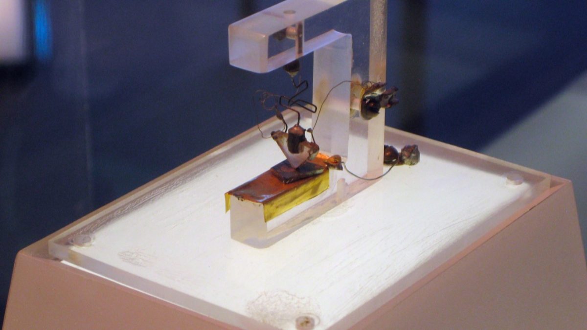
Brattain and Bardeen focused on the surface physics of semiconductors. On December 16, 1947, Brattain shaped a microscopic wedge of polystyrene plastic, wrapped a ribbon of gold foil around it, and sliced the gold foil at the apex with a razor blade to create two parallel gold contacts separated by just 50 micrometers ($0.002\text{ inches}$).
Pressing this plastic wedge firmly onto a slab of polycrystalline Germanium sitting on a metal baseplate, Brattain connected one contact (the Emitter) and the second contact (the Collector). When a tiny electric current was applied to the emitter, it flooded the germanium surface with positive charge carriers (“holes”), dramatically modulating a far larger current flowing to the collector:
$$\Delta I_c = \alpha \cdot \Delta I_e, \quad \alpha \approx 1$$They had invented the point-contact transistor (short for *transfer-resistor*). It amplified audio signals by 18-fold and switched states in nanoseconds without generating heat or requiring warmup time. For this epochal discovery, Bardeen, Brattain, and Shockley were awarded the 1956 Nobel Prize in Physics.
2. Shockley Semiconductor and the Traitorous Eight
William Shockley, driven by fierce commercial ambition, moved to Mountain View, California in 1956 to establish Shockley Semiconductor Laboratory, seeking to commercialize silicon transistors in his hometown. Shockley was a brilliant physicist but a paranoid, tyrannical manager.
In September 1957, eight of Shockley’s brilliant young scientists and engineers—Robert Noyce, Gordon Moore, Julius Blank, Victor Grinich, Jean Hoerni, Eugene Kleiner, Jay Last, and Sheldon Roberts—resigned in protest. Shockley famously branded them the “Traitorous Eight”.
Securing \$1.3 million in backing from industrialist Sherman Fairchild, the group founded Fairchild Semiconductor in Santa Clara Valley. This rebellion created the blueprint for venture-backed technological enterprise and gave birth to Silicon Valley.
3. The Integrated Circuit: Kilby and Noyce
Even with miniature transistors, circuits were still hand-soldered point-to-point on printed circuit boards. Two men independently solved this manufacturing bottleneck:
- Jack Kilby (Texas Instruments, July 1958): While the rest of the laboratory was on summer vacation, Kilby built the first working microchip on a single wafer of Germanium. By integrating a transistor, capacitor, and three resistors on the same crystal slab and linking them with flying gold wires, Kilby proved that all circuit components could be made of the same semiconductor material.
- Robert Noyce (Fairchild Semiconductor, January 1959): Building upon Jean Hoerni’s planar process (which used silicon dioxide passivation and photolithography to etch transistors onto flat silicon wafers), Noyce introduced printed aluminum interconnects evaporated directly onto the silicon surface. Noyce’s monolithic planar integrated circuit could be mass-produced through optical photographic printing, making microchips dirt cheap and extraordinarily reliable.
| Generation | Active Component | Switching Time | Failure Rate / Cost |
|---|---|---|---|
| 1st Gen (1940s) | Thermionic Vacuum Tubes | $10^{-5}\text{ s}$ ($10\text{ }\mu\text{s}$) | High burnout rate; \$5–10 per tube; 150 kW power |
| 2nd Gen (1950s) | Discrete Germanium Transistors | $10^{-7}\text{ s}$ ($100\text{ ns}$) | Rugged; \$1–5 per unit; milliwatts of power |
| 3rd Gen (1960s) | Planar Silicon Integrated Circuits | $10^{-9}\text{ s}$ ($1\text{ ns}$) | Extremely reliable; pennies per gate via lithography |
| 4th Gen (1970s+) | Microprocessors (VLSI / FinFET) | $< 10^{-11}\text{ s}$ ($< 10\text{ ps}$) | Billions of transistors per die for fractions of a cent |
4. Moore’s Law: The Engine of Modern Civilization
In April 1965, for the 35th-anniversary issue of Electronics magazine, Fairchild’s director of R&D Gordon Moore wrote a four-page article titled “Cramming more components onto integrated circuits”. Examining empirical data from 1959 to 1965, Moore observed that the number of components on an integrated circuit at minimum manufacturing cost had doubled every year, and projected this exponential curve would continue for at least a decade.
In 1975, Moore revised the doubling cadence to approximately every two years:
$$N(t) = N_0 \cdot 2^{\frac{t – t_0}{2}}$$Moore’s Law was not a natural law of physics; it was a self-fulfilling economic and engineering pact. Semiconductor roadmaps worldwide aligned billions of dollars in capital expenditure, extreme ultraviolet (EUV) lithography, and material science to meet Moore’s pace. Dennard scaling (which held that power density remained constant as transistors shrank) powered this exponential climb for four decades, transforming computers from room-sized mainframes into microscopic supercomputers resting in the palm of every human hand.
Primary Academic References
- Bardeen, J., & Brattain, W. H. (1948). The Transistor, A Semi-Conductor Triode. Physical Review, 74(2), 230–231.
- Kilby, J. S. (1976). Invention of the integrated circuit. IEEE Transactions on Electron Devices, 23(7), 648–654.
- Noyce, R. N. (1961). Semiconductor device-and-lead structure. US Patent 2,981,877.
- Moore, G. E. (1965). Cramming more components onto integrated circuits. Electronics, 38(8), 114–117.