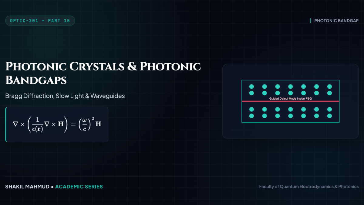
In solid-state physics, the periodic spatial electrostatic potential of an atomic crystal lattice gives rise to electronic energy bandgaps: energy intervals where electron wavefunctions cannot propagate, creating semiconductors and insulators. In 1987, Eli Yablonovitch and Sajeev John recognized a historic mathematical symmetry: if dielectric permittivity is patterned periodically on the scale of optical wavelengths, destructive interference creates a Photonic Bandgap (PBG)—a frequency window wherein photons are completely forbidden from propagating in any direction, permitting unprecedented spatial and temporal confinement of light.
1. Bloch-Floquet Electromagnetism and Master Wave Equation
Consider an inhomogeneous, lossless, non-magnetic dielectric medium where the relative permittivity is periodically modulated across a spatial lattice (mathbf{R}): (psilon(mathbf{r} + mathbf{R}) = psilon(mathbf{r})). Substituting time-harmonic fields into Maxwell’s curl equations yields the Hermitian master eigenvalue equation for the magnetic field (mathbf{H}(mathbf{r})):
[
abla imes left( rac{1}{psilon(mathbf{r})}
abla imes mathbf{H}(mathbf{r})
ight) = left( rac{omega}{c}
ight)^2 mathbf{H}(mathbf{r})
]
By the Bloch-Floquet Theorem, the eigensolutions are plane waves modulated by a lattice-periodic vector function (mathbf{u}_{mathbf{k}}(mathbf{r})):
[
mathbf{H}_{mathbf{k}}(mathbf{r}) = e^{i mathbf{k} cdot mathbf{r}} mathbf{u}_{mathbf{k}}(mathbf{r}) quad ext{where} quad mathbf{u}_{mathbf{k}}(mathbf{r} + mathbf{R}) = mathbf{u}_{mathbf{k}}(mathbf{r})
]
Solving this eigenvalue problem across the irreducible Brillouin zone maps out the photonic band structure (omega_n(mathbf{k})). When dielectric contrast (Delta psilon = psilon_{ ext{high}} / psilon_{ ext{low}}) is sufficiently high (typically (Delta psilon > 4 ext{–}8)), a complete three-dimensional Photonic Bandgap opens, barring all electromagnetic propagation regardless of polarization.
2. Engineering Light via Structural Defects
Just as doping atomic semiconductors creates localized donor/acceptor electronic states inside the bandgap, selectively altering the periodicity of a photonic crystal creates localized optical states:
- Point-Defect Cavities (0D Confinement): Removing a single hole (or modifying its radius) in a 2D photonic crystal slab forms an optical nanocavity. Because light within the PBG cannot escape laterally into the lattice and is trapped vertically by total internal reflection, quality factors exceed (Q > 10^6) while mode volume shrinks to the sub-cubic-wavelength scale ((V_{ ext{mode}} sim 0.05 (lambda/n)^3)), yielding unprecedented Purcell enhancement.
- Line-Defect Waveguides (1D Confinement): Omitting an entire row of holes creates a defect waveguiding channel. Light is forced to follow the waveguide around sharp sub-micrometer bends with zero radiation loss, forming ultra-compact on-chip photonic routing networks.
3. Slow Light and Enhanced Optical Non-Linearity
At the edges of the photonic bandgap, the dispersion relation flattens dramatically ((partial omega / partial k o 0)). The optical group velocity drops precipitously:
[
v_g = rac{partial omega}{partial k} = rac{c}{n_g} ll c
]
where (n_g) is the group index, which can exceed (n_g > 100 ext{–}1000). Under slow-light propagation, optical energy is compressed spatially: the local energy density scales as (u propto I / v_g). This colossal field concentration enhances non-linear optical phase shifts, Raman scattering, and four-wave mixing efficiencies by a factor of (n_g^2), enabling non-linear switching at milliwatt power thresholds.